Welcome to our comprehensive guide on Designing Sequential Circuits through Verilog HDL. While combinational logic forms the foundation of digital systems, sequential circuits introduce memory elements, enabling the creation of complex and dynamic digital systems. These circuits are pivotal in applications like processors, memory units, and state machines. Whether you’re a student, hobbyist, or professional, mastering sequential circuit design in Verilog is essential for advancing in digital electronics and VLSI design. Let’s delve into the essentials of sequential circuits, their classifications, and practical Verilog implementations.
Sequential Versus Combinational Circuits
Understanding the distinction between sequential and combinational circuits is fundamental in digital electronics. While combinational circuits produce outputs solely based on current inputs, sequential circuits consider both current inputs and past states, thanks to their memory elements. This historical dependency allows sequential circuits to perform tasks that require data storage, synchronization, and control flow, making them indispensable in modern digital systems.
Synchronous Sequential Circuits
Synchronous sequential circuits operate in tandem with a clock signal, ensuring that state transitions occur at precise intervals. The clock acts as a metronome, coordinating the timing of operations across the circuit. This synchronization enhances reliability and predictability, making synchronous circuits ideal for applications requiring precise timing, such as CPUs and digital communication systems.
Key Characteristics:
- Clock-Driven: State changes occur on clock edges (rising or falling).
- Predictable Timing: Synchronization with the clock ensures consistent performance.
- Edge-Triggered Flip-Flops: Common memory elements used for state storage.
Asynchronous Sequential Circuits
In contrast, asynchronous sequential circuits do not rely on a clock signal. Instead, their state changes are triggered by changes in input signals. While this can lead to faster operations since state transitions can occur immediately, it also introduces challenges like race conditions and hazards, making these circuits harder to design and debug. Asynchronous circuits are typically used in applications where speed is critical and precise timing can be managed effectively.
Key Characteristics:
- Event-Driven: State changes occur in response to input signal changes.
- Potential for High Speed: Immediate response to inputs can reduce latency.
- Complex Design: Managing timing and avoiding race conditions requires meticulous design.
Latches and Flip-Flops
At the heart of sequential circuits are latches and flip-flops, the fundamental memory elements that store binary data. While both serve to hold state information, they differ in their triggering mechanisms and operational behaviors.
Difference Between Latches and Flip-Flops
The primary distinction lies in how they are triggered:
- Latches: Level-Triggered devices that respond to input changes as long as the enable signal is active.
- Flip-Flops: Edge-Triggered devices that respond only to transitions (rising or falling edges) of the clock signal.
This difference impacts their usage; latches are simpler but can introduce timing complexities, whereas flip-flops offer more precise control, making them preferable in synchronous designs.
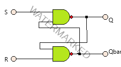
S-R Latch
The S-R Latch is the simplest form of a latch, constructed using two cross-coupled NAND or NOR gates. It has two inputs: Set (S) and Reset (R), and two outputs: Q and Qbar. While straightforward, the S-R latch has a forbidden state when both S and R are active simultaneously, leading to undefined outputs.
Truth Table
| S | R | Qn+1 | State |
|---|---|---|---|
| 0 | 0 | x | Forbidden |
| 0 | 1 | 1 | Set |
| 1 | 0 | 0 | Reset |
| 1 | 1 | Qn | Hold |
When both S and R are inactive (1 for NOR-based latches or 0 for NAND-based), the latch holds its previous state. Activating S sets the output, while activating R resets it. However, activating both simultaneously leads to an invalid state, emphasizing the need for careful input management.
Design
Here’s the Verilog implementation of an S-R Latch using NAND gates:
module SR_latch(
        input S,
        input R,
        output Q,
        output Qbar
    );
        nand n1(Q, S, Qbar);
        nand n2(Qbar, R, Q);
    endmodule
Test Bench
To verify the functionality of the S-R Latch, use the following test bench:
module SR_latch_tb;
        reg S;
        reg R;
        wire Q;
        wire Qbar;

        SR_latch uut (.S(S), .R(R), .Q(Q), .Qbar(Qbar));

        initial begin
            $monitor("Time=%0t | S=%b, R=%b | Q=%b, Qbar=%b", $time, S, R, Q, Qbar);
            // Initialize inputs
            S = 1; R = 1; #10;
            // Test Set
            S = 0; R = 1; #10;
            // Test Reset
            S = 1; R = 0; #10;
            // Test Hold
            S = 1; R = 1; #10;
            // Test Forbidden
            S = 0; R = 0; #10;
        end

        initial begin
            $dumpfile("SR_latch_tb.vcd");
            $dumpvars;
        end
    endmodule

S-R Flip-Flop
The S-R Flip-Flop enhances the basic S-R latch by incorporating a clock signal, making it edge-triggered. This design mitigates the forbidden state issue inherent in the S-R latch by ensuring that state changes occur only on specific clock transitions, typically the rising or falling edge.

Truth Table
| Clock | S | R | Qn+1 | State |
|---|---|---|---|---|
| 1 | 0 | 0 | Qn | Hold |
| 1 | 0 | 1 | 0 | Reset |
| 1 | 1 | 0 | 1 | Set |
| 1 | 1 | 1 | x | Invalid |
By synchronizing state changes with the clock’s edge, the S-R Flip-Flop ensures stability and predictability, essential for reliable digital system operation. However, the invalid state when both S and R are active simultaneously still poses challenges, which are addressed in more advanced flip-flop designs like the J-K Flip-Flop.
Design
Here’s the Verilog implementation of an S-R Flip-Flop:
module SR_flip_flop(
        input S,
        input R,
        input clk,
        output reg Q,
        output reg Qbar
    );
        always @(posedge clk) begin
            if (!S && R)
                Q <= 0;
            else if (S && !R)
                Q <= 1;
            else if (!S && !R)
                Q <= Q;
            // When S and R are both 1, it's an invalid state; no action taken
        end
        always @(*) begin
            Qbar = ~Q;
        end
    endmodule
Test Bench
To verify the S-R Flip-Flop, use the following test bench:
module SR_flip_flop_tb;
        reg S;
        reg R;
        reg clk;
        wire Q;
        wire Qbar;

        SR_flip_flop uut (.S(S), .R(R), .clk(clk), .Q(Q), .Qbar(Qbar));

        initial begin
            $monitor("Time=%0t | S=%b, R=%b, clk=%b | Q=%b, Qbar=%b", $time, S, R, clk, Q, Qbar);
            // Initialize inputs
            S = 1; R = 1; clk = 0; #10;
            // Toggle clock
            forever #5 clk = ~clk;
        end

        initial begin
            #10 S = 0; R = 1; // Reset
            #10 S = 1; R = 0; // Set
            #10 S = 1; R = 1; // Invalid
            #10 S = 0; R = 0; // Hold
            #10 $finish;
        end

        initial begin
            $dumpfile("SR_flip_flop_tb.vcd");
            $dumpvars;
        end
    endmodule

J-K Flip-Flop
The J-K Flip-Flop is an evolution of the S-R Flip-Flop, eliminating the invalid state by introducing two new inputs: J and K. By connecting the S and R inputs to the J and K inputs respectively through appropriate logic, the J-K Flip-Flop can toggle its state without ambiguity.

Truth Table
| Clock | J | K | Qn+1 | State |
|---|---|---|---|---|
| 1 | 0 | 0 | Qn | Hold |
| 1 | 0 | 1 | 0 | Reset |
| 1 | 1 | 0 | 1 | Set |
| 1 | 1 | 1 | ~Qn | Toggle |
The J-K Flip-Flop’s ability to toggle its state when both J and K are active removes the ambiguity present in the S-R Flip-Flop, making it a more versatile and widely used memory element in digital systems.
Design
Here’s the Verilog implementation of a J-K Flip-Flop:
module JK_flip_flop(
        input J,
        input K,
        input clk,
        output reg Q,
        output Qbar
    );
        assign Qbar = ~Q;

        always @(posedge clk) begin
            case({J, K})
                2'b00: Q <= Q;          // Hold
                2'b01: Q <= 0;          // Reset
                2'b10: Q <= 1;          // Set
                2'b11: Q <= ~Q;         // Toggle
            endcase
        end
    endmodule
Test Bench
To verify the J-K Flip-Flop, use the following test bench:
module JK_flip_flop_tb;
        reg J;
        reg K;
        reg clk;
        wire Q;
        wire Qbar;

        JK_flip_flop uut (.J(J), .K(K), .clk(clk), .Q(Q), .Qbar(Qbar));

        initial begin
            $monitor("Time=%0t | J=%b, K=%b, clk=%b | Q=%b, Qbar=%b", $time, J, K, clk, Q, Qbar);
            // Initialize inputs
            J = 0; K = 0; clk = 0; #10;
            // Toggle clock
            forever #5 clk = ~clk;
        end

        initial begin
            #10 J = 1; K = 0; // Set
            #10 J = 0; K = 1; // Reset
            #10 J = 1; K = 1; // Toggle
            #10 J = 0; K = 0; // Hold
            #10 $finish;
        end

        initial begin
            $dumpfile("JK_flip_flop_tb.vcd");
            $dumpvars;
        end
    endmodule

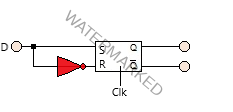
D Flip-Flop
The D Flip-Flop simplifies the Flip-Flop design by eliminating the invalid state. It captures the value of the data input D at a specific clock edge and holds it until the next clock event. This straightforward behavior makes the D Flip-Flop a staple in digital circuit design, especially in shift registers and memory modules.
Truth Table
| Clock | D | Qn+1 |
|---|---|---|
| 0 | x | Qn |
| 1 | 0 | 0 |
| 1 | 1 | 1 |
The D Flip-Flop ensures that the output Q mirrors the input D precisely at each clock edge, maintaining data integrity across digital systems.
Design
Here’s the Verilog implementation of a D Flip-Flop:
module D_flip_flop(
        input clk,
        input D,
        output reg Q,
        output Qbar
    );
        assign Qbar = ~Q;

        always @(posedge clk) begin
            Q <= D;
        end
    endmodule
Test Bench
To verify the D Flip-Flop, use the following test bench:
module D_flip_flop_tb;
        reg clk;
        reg D;
        wire Q;
        wire Qbar;

        D_flip_flop uut (.clk(clk), .D(D), .Q(Q), .Qbar(Qbar));

        initial begin
            $monitor("Time=%0t | clk=%b, D=%b | Q=%b, Qbar=%b", $time, clk, D, Q, Qbar);
            // Initialize inputs
            clk = 0; D = 0; #10;
            // Toggle clock
            forever #5 clk = ~clk;
        end

        initial begin
            #10 D = 1; #10;
            D = 0; #10;
            D = 1; #10;
            D = 1; #10;
            D = 0; #10;
            $finish;
        end

        initial begin
            $dumpfile("D_flip_flop_tb.vcd");
            $dumpvars;
        end
    endmodule

T Flip-Flop
The T Flip-Flop is a specialized form of the J-K Flip-Flop, where the inputs J and K are tied together. Its primary function is to toggle the output state on each clock pulse when the T input is active. This behavior is particularly useful in creating toggle switches, counters, and frequency dividers.
| Clock | T | Qn+1 |
|---|---|---|
| 0 | x | Qn |
| 1 | 0 | Qn |
| 1 | 1 | ~Qn |
Design
Here’s the Verilog implementation of a T Flip-Flop:
module T_flip_flop(
        input clk,
        input T,
        output reg Q,
        output Qbar
    );
        assign Qbar = ~Q;

        always @(posedge clk) begin
            if (T)
                Q <= ~Q;
            else
                Q <= Q;
        end
    endmodule
Test Bench
To verify the T Flip-Flop, use the following test bench:
module T_flip_flop_tb;
        reg clk;
        reg T;
        wire Q;
        wire Qbar;

        T_flip_flop uut (.clk(clk), .T(T), .Q(Q), .Qbar(Qbar));

        initial begin
            $monitor("Time=%0t | clk=%b, T=%b | Q=%b, Qbar=%b", $time, clk, T, Q, Qbar);
            // Initialize inputs
            clk = 0; T = 0; #10;
            // Toggle clock
            forever #5 clk = ~clk;
        end

        initial begin
            #10 T = 1; #10;
            T = 0; #10;
            T = 1; #10;
            T = 1; #10;
            T = 0; #10;
            $finish;
        end

        initial begin
            $dumpfile("T_flip_flop_tb.vcd");
            $dumpvars;
        end
    endmodule

Race Around Condition
The race around condition is a phenomenon in asynchronous and some synchronous flip-flop designs where the output toggles multiple times during a single clock pulse. This occurs due to feedback paths that allow the output to change repeatedly while the clock signal remains active, leading to unpredictable and unstable behavior.
To mitigate race around conditions, designers often use master-slave flip-flop configurations or incorporate edge-triggered mechanisms that ensure state changes occur only once per clock cycle. Properly addressing this issue is crucial for maintaining data integrity and ensuring reliable circuit operation.
Best Practices in Verilog Modeling
To design efficient and reliable sequential circuits using Verilog, adhere to the following best practices:
- Consistent Naming Conventions: Use clear and descriptive names for modules, signals, and instances to enhance code readability.
- Modular Design: Break down complex circuits into smaller, reusable modules, promoting scalability and maintainability.
- Comprehensive Documentation: Comment your code to explain functionality, logic, and design decisions, aiding future reviews and collaborations.
- Utilize Verilog Libraries: Leverage existing libraries for standard components to save time and reduce errors.
- Thorough Testing: Develop extensive test benches to simulate various scenarios, ensuring your designs behave as expected under all conditions.
- Stay Updated with Latest Verilog Standards: Incorporate modern Verilog features and methodologies to enhance design efficiency and compatibility.
Latest Trends in Sequential Circuit Design and Verilog
The landscape of sequential circuit design and Verilog HDL is continually evolving. Here are some of the latest trends shaping the industry:
- SystemVerilog Integration: An extension of Verilog, SystemVerilog offers advanced features for design and verification, making it a preferred choice for complex digital systems.
- High-Level Synthesis (HLS): Tools that convert high-level programming languages like C++ into Verilog, accelerating the design process and enabling rapid prototyping.
- Hardware Security: Incorporating security features in sequential circuits to protect against hardware-based attacks, ensuring data integrity and system reliability.
- Low-Power Design Techniques: Emphasizing power efficiency in sequential circuit design to extend battery life and reduce thermal output in portable and embedded systems.
- Advanced FPGA Utilization: Leveraging the latest FPGA technologies for implementing sophisticated sequential circuits, enabling high-performance and flexible digital systems.
Staying abreast of these trends ensures that your sequential circuit designs remain cutting-edge, efficient, and secure.
Conclusion
In this article, we’ve delved into the realm of Designing Sequential Circuits through Verilog HDL, covering essential concepts like the differences between sequential and combinational circuits, various types of latches and flip-flops, and addressing critical issues like the race around condition. By mastering these elements and adhering to best practices, you can design robust and efficient sequential circuits tailored to modern digital systems. Embracing the latest trends and continuously refining your Verilog skills will further enhance your proficiency in digital circuit design. For more insightful articles and up-to-date information on digital electronics and circuit design, stay connected with Gossipfunda.
Don’t Miss Our Previous Blogs
- Non-Arithmetic Combinational Circuits
- Designing Combinational Circuits through Verilog HDL
- Modeling of Combinational Logic Circuits
- Modeling of Universal and Special Gates on Verilog
I am an electronics and communication graduate. I qualified GATE in the same domain in 2019. Due to the appetite for VLSI, I am going to join the Hong Kong University of Science and Technology for Masters in IC design this year. My interest in writing evoked during college time when I wrote technical essays for college fest. Apart from it, I am a part of a few local NGOs too.