Modeling of Universal and Special Gates on Verilog
In this write-up, we discuss the remaining Gates, which structure the foundation of Digital Electronics, i.e., Modeling of Universal and Special Gates on Verilog. We have already covered each topic related to it. So visit them all in Verilog Catagory.
See the first part: Modeling Basic Gates through Verilog
Universal Gates
The NAND gate and NOR gate are called Universal gates because they can perform all the three essential functions of AND, OR, and NOT gates. Furthermore, these two gates realize all other gates.
NAND Gate
The NAND gate is an AND gate followed by NOT gate. Thus, we can say it is a NOT-AND operation. It may have two or more inputs but only one output. Below is the logical symbol of a NAND gate and the truth table.

| Input A | Input B | Output C |
| 0 | 0 | 1 |
| 0 | 1 | 1 |
| 1 | 0 | 1 |
| 1 | 1 | 0 |
The logic expression of output is C= (A.B)’ = A’ +B’ (by de morgan’s theorem)
It is clear from the truth table of the two-input NAND gate that the output is High when either A or B or when both the inputs are Low. We can say that, if both A’ and B’ are High, then the output is High. Therefore, the NAND gate can perform the OR function by inverting the inputs and then ORing it. In conclusion, the NAND Gate and AND Gate are complementary for a given number of inputs. The OR gate with inverted inputs is called bubbled OR gate or negative OR gate. The NAND gate is also called an active low OR gate.
Design Module
//Gate Level Modeling
module nandgate(output reg c, input a,b);
nand  a1(c,a,b);
endmodule
//Data Flow Modeling
module nandgate (output reg c, input a,b); // data type can be declared in port list
assign c = ~(a & b); // (~) is the symbol for inverter
endmodule//Behavioral Modeling
module nandgate(c,a,b);
output reg c;
input a,b;
always@ (*) // can be replaced by always@(a or b)
begin
if(a==1 && b==1)
begin
c=0;
end
else
c=1;
end
endmoduleTest Bench
module nandgate_tb;
wire t_c;
reg t_a,t_b;
nandgate dut(t_c, t_a, t_b);
initial               // can be used with single function
$monitor(t_a,t_b,t_c);
initial
$display("a=%b, b=%b ,c=%b",t_a,t_b,t_c); // same as printf in C programming
                                             language
initial  //can be used with clubbed functions
begin
$dumpfile("dump.vcd");
$dumpvars;
end
initial
begin
t_a=0;
t_b=0;
#50
t_a=0;
t_b=1;
#50
t_a=1;
t_b=0;
#50
t_a=1;
t_b=1;
end
endmodule
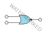
NOR Gate
OR gate and NOT gate merges to make NOR Gate. So we can say it is a NOT-OR operation. It may certainly have two or more inputs and an output. Listed below are the symbol and the truth table of the gate.

| Input A | Input B | Output C |
| 0 | 0 | 1 |
| 0 | 1 | 0 |
| 1 | 0 | 0 |
| 1 | 1 | 0 |
Truth table clears that the output is one’ only if all the inputs are at logic zero. We can also say that if the inputs A’ =B’ =High, then the output C is High. Thus, the NOR gate is equivalent to AND gate with inverted inputs, and it can be realized by a bubbled AND gate. Active LOW AND gate is the other name for the NOR gate.
The logical expression for the output is
C = (A+B)’ = A’.B’
Design Module
//Gate level modelling
module norgate(output reg c, input a,b);
nor  a1(c,a,b);
endmodule
//Data flow modeling
module norgate (output reg c, input a,b);
assign c = ~(a + b);
endmodule//Behavioral Modeling
module norgate(c,a,b);
output reg c;
input a,b;
always@ (*)
begin
if(a==0 && b==0)
begin
c=1;
end
else
c=0;
end
endmoduleTest Bench
module norgate_tb;
wire t_c;
reg t_a,t_b;
norgate dut(t_c, t_a, t_b);
initial
begin
$monitor(t_a,t_b,t_c);
$display("a=%b, b=%b ,c=%b",t_a,t_b,t_c);
$dumpfile("dump.vcd");
$dumpvars;
end
initial
begin
t_a=0;
t_b=0;
#50
t_a=0;
t_b=1;
#50
t_a=1;
t_b=0;
#50
t_a=1;
t_b=1;
end
endmodule
The Exclusive OR gate and Exclusive NOR gate is known as Special function gates. Though they can be realized using Universal gates, their unique application in electronics make them special.
EX-OR Gate
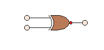
A basic EX-OR gale is a two-input single-output logic gate whose output is assumed to be HIGH only when it’s one of the inputs is High. The logic symbol and the truth table for a two-input EX-OR gate are shown respectively.

| Input A | Input B | Output C |
| 0 | 0 | 0 |
| 0 | 1 | 1 |
| 1 | 0 | 1 |
| 1 | 1 | 0 |
If the input variables are represented by A and B, then the logical expression for output is C=A’B+AB’ = A ⊕ B
Practically, three or more input EX-OR gate does not exist. But when more than two variables are EXORed, a number of two input EX-OR gate is used. There, the output is assumed to be one when an odd number of input variables is one. That is why the Ex-OR gate is known as the odd number of one’s detector in the input. The most crucial application of the EX-OR gate is in ‘parity generation and detection. It is also known as the “staircase switch.”
Design Module
//Gate Level Modeling
module exor(output reg c, input a,b);
xor a1(c,a,b);
endmodule
//Data Flow Modeling
module exor(output reg c, input a,b);
assign c = a^b;
endmodule//Behavioral Modeling
module exor(c,a,b);
output reg c;
input a,b;
always@ (*)
begin
if(a==b)
begin
c=0;
end
else
c=1;
end
endmoduleTest Bench
module exor_tb;
wire t_c;
reg t_a,t_b;
exor dut(t_c, t_a, t_b);
initial
$monitor(t_a,t_b,t_c);
initial
$display("a=%b, b=%b ,c=%b",t_a,t_b,t_c);
initial
begin
$dumpfile("dump.vcd");
$dumpvars;
end
initial
begin
t_a=0;
t_b=0;
#50
t_a=0;
t_b=1;
#50
t_a=1;
t_b=0;
#50
t_a=1;
t_b=1;
end
endmodule
EX-NOR Gate
Modeling of Universal and Special Gates EX-NOR on Verilog. An EX-NOR gate is an EX-OR gate followed by NOT gate. The EX-NOR gate is two inputs and one output logic circuit in which the output is 1 only when both the inputs are the same. Thus, it is also called as “gate of equivalence” or “coincidence logic”. Diagram and truth table of two-input EX-NOR gate are shown.

| Input A | Input B | Output C |
| 0 | 0 | 1 |
| 0 | 1 | 0 |
| 1 | 0 | 0 |
| 1 | 1 | 1 |
Thus, for input variables A and B the logical expression for the output of an EX-NOR gate is given, C = AB+ A’B’ =A ʘ B
Practically, three or more variable EX-NOR gate does not exist. However, if the number of variables has to be EX-NORED, then a number of two variable EX-NOR gates will be used in which the output is high for even number of input variables is one. Thus, it is also known as “even number of one’s detector”. When the number of input variables is odd, then it is also known as an “odd number of one’s detector”.
Design Module
//Gate Level Modeling Special Gates through Verilog
module exnor(output reg c, input a,b);
xnor a1(c,a,b);
endmodule
//Data Flow Modeling
module exnor(output reg c, input a,b);
assign c = ~(a ^ b);
endmodule//Behavioral Modeling
module exnor(c,a,b);
output reg c;
input a,b;
always@ (*)
begin
if(a==b)
begin
c=1;
end
else
c=0;
endTest Bench
module exnor_tb;
wire t_c;
reg t_a,t_b;
exnor dut(t_c, t_a, t_b);
initial
$monitor(t_a,t_b,t_c);
initial
$display("a=%b, b=%b ,c=%b",t_a,t_b,t_c);
initial
begin
$dumpfile("dump.vcd");
$dumpvars;
end
initial
begin
t_a=0;
t_b=0;
#50
t_a=0;
t_b=1;
#50
t_a=1;
t_b=0;
#50
t_a=1;
t_b=1;
end
endmodule
BUFFER
In novice language, a buffer means a temporary barrier. Its application certainly remains the same in digital electronics. A buffer is used to transfer a signal from input to output unchanged. In other words, it is the opposite of the inverter. However, the output will be the same as the input and use to increase the propagation delay.

| Input a | Output b |
| 0 | 0 |
| 1 | 1 |
Design Module
module bufdes(y,a);
input a;
output reg b;
assign b = a;
endmodule
Test Bench
module buf_tb;
reg a;
wire b;
bufdes dut(b,a);
initial
begin
$display (a,b);
$monitor(a,b);
$dumpfile("dump.vcd");
$dumpvars;
end
endmodule
Transmission Gate
Firstly, we shall see the basics of CMOS. A complementary MOSFET is a combination of p-type MOSFET and n-type MOSFET. Term complimentary here means using complementary MOSFETs to perform a logical operation. CMOS devices are popular because they have high speed, low power consumption, and noise immunity.
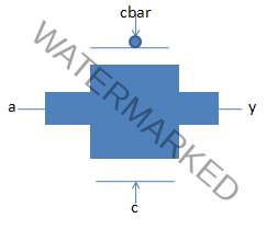
Transmission door (TG) or pass gate is a basic switch circuit comprising of one NMOS and one PMOS transistor, associated in equal. Complementary gate voltages are applied to both the transistors.
The TG works as a bidirectional switch between the hubs A and B. Additionally, signal C constrains them. In the event that the control signal C is logic high, i.e., equivalent to voltage – at that point, the two transistors are turned on and give a low resistance current way between the hubs A and B. In the event that the control signal C is low, at that point the two transistors will be off, and the way between the hubs A and B will be an open circuit.

| Control | Input a | Output y | |
| pMOS | nMOS | ||
| 0 | 1 | 0 | 0 |
| 1 | 1 | ||
| 1 | 0 | 0 | z |
| 1 | z |
‘z’ signifies high impedance or infinitely high resistance.
Design Module
module transgate(y,c,a);
output reg y;
input a,c ;
input wire cbar;
assign cbar = ~c;
cmos cm(y,a,c,cbar);
endmodule
Cmos is already declared in the Verilog. NMOS and PMOS combine to make CMOS. So, the code line CMOS
CMOS cm (y, a, c, cbar); has the below alternate way of modeling as:
nmos(y, a, c);
pmos (y, a, cbar);
Test Bench
module transmissiongatetb;
wire y;
reg a,c;
transgate dut(y,c,a);
initial
begin
$display ("\ta\ty",a,y);
a = 0; c = 0; # 50
a = 1; c = 0; # 50
a =0; c = 1; # 50
a = 1; c = 1;
end
//enabling the wave dump
initial
begin
$dumpfile("dump.vcd");
$dumpvars;
end
endmodule
Conclusion
In this very article: Modeling of Universal and Special Gates on Verilog, we learned about the Universal and Special Purpose gates and justified why they are named so. Additionally, we saw two other gates which have more application in advanced electronics and VLSI. From the next article, we will design the Combinational Circuit.
I am an electronics and communication graduate. I qualified GATE in the same domain in 2019. Due to the appetite for VLSI, I am going to join the Hong Kong University of Science and Technology for Masters in IC design this year. My interest in writing evoked during college time when I wrote technical essays for college fest. Apart from it, I am a part of a few local NGOs too.


Pingback: Modeling of Combinational Logic Circuits - gossipfunda