Welcome to our in-depth guide on Designing or Modeling of Combinational Circuits through Verilog HDL. In our previous article, we explored arithmetic combinational circuits. Combinational circuits are the backbone of digital electronics, finding applications in Arithmetic Logic Units (ALUs), processors, and various other digital systems. This guide delves into essential combinational circuits, providing detailed Verilog designs and practical examples to enhance your understanding and skills.
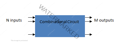
Combinational circuits process ‘n’ input binary variables from external sources and produce ‘m’ output variables through internal logic configurations. Each input and output exists as an analog signal interpreted as binary logic levels—’1′ (HIGH) and ‘0’ (LOW). Understanding these circuits lays the foundation for more complex digital systems, such as Arithmetic Logic Units (ALUs) and microprocessors.
Do not Miss: Modeling of Universal and Special Gates on Verilog
Half-Adder
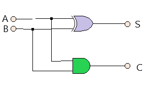
The Half Adder is a fundamental arithmetic circuit that adds two single-bit binary numbers. It has two inputs, designated as augend (A) and addend (B), and produces two outputs: Sum (S) and Carry (C). The Sum represents the least significant bit of the addition, while the Carry indicates an overflow to the next higher bit.
| A | B | Sum | Carry |
| 0 | 0 | 0 | 0 |
| 0 | 1 | 1 | 0 |
| 1 | 0 | 1 | 0 |
| 1 | 1 | 0 | 1 |
From the truth table, we derive the Boolean expressions for Sum and Carry:
- Sum (S): S = A’B + AB’ = A ⊕ B
- Carry (C): C = AB
These expressions can be implemented using XOR and AND gates. The Half Adder is essential in building more complex adders and arithmetic circuits.
Design Module
Below is the Verilog code for a Half Adder using different modeling approaches:
// Gate Level Modeling
module ha(s, c, a, b);
    output reg s, c;
    input a, b;
    xor G1(s, a, b);
    and G2(c, a, b);
endmodule
// Data Flow Modeling
module ha(a, b, s, c);
    input a, b;
    output s, c;
    assign s = a ^ b;
    assign c = a & b;
endmodule
// Behavioral Modeling
module ha_behav(s, c, a, b);
    output reg s, c;
    input a, b;
    always @(*) begin
        s = a ^ b;
        c = a & b;
    end
endmodule
Test Bench
To verify the functionality of the Half Adder, we use the following test bench:
module ha_tb;
    reg a, b;
    wire s, c;
    ha_behav dut(s, c, a, b);

    initial begin
        $monitor("A=%b, B=%b | Sum=%b, Carry=%b", a, b, s, c);
        $dumpfile("ha_tb.vcd");
        $dumpvars;

        // Test cases
        a = 0; b = 0; #100;
        a = 0; b = 1; #100;
        a = 1; b = 0; #100;
        a = 1; b = 1; #100;
    end
    endmodule

Full Adder
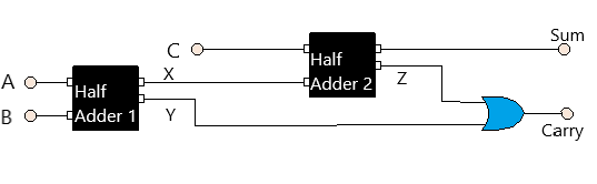
The Full Adder extends the functionality of the Half Adder by including an additional input for carry-in (C_in). This allows the Full Adder to add three single-bit numbers, producing a Sum (S) and a Carry-Out (C_out). Full Adders are crucial for constructing multi-bit adders used in processors and other digital systems.
| A | B | C_in | Sum | C_out |
| 0 | 0 | 0 | 0 | 0 |
| 0 | 0 | 1 | 1 | 0 |
| 0 | 1 | 0 | 1 | 0 |
| 0 | 1 | 1 | 0 | 1 |
| 1 | 0 | 0 | 1 | 0 |
| 1 | 0 | 1 | 0 | 1 |
| 1 | 1 | 0 | 0 | 1 |
| 1 | 1 | 1 | 1 | 1 |
The Boolean expressions derived from the truth table are:
- Sum (S): S = A ⊕ B ⊕ C_in
- Carry-Out (C_out): C_out = AB + BC_in + CA
These expressions can be implemented using XOR, AND, and OR gates, or by cascading Half Adders as shown in the diagram above. Full Adders are the building blocks for constructing n-bit adders.
Design Module
Here is the Verilog code for a Full Adder using Half Adders:
// Full Adder using Half Adders
module fa(sum, carry, a, b, c_in);
    output reg sum, carry;
    input a, b, c_in;
    wire s1, c1, c2;

    ha ha1(s1, c1, a, b);      // First Half Adder
    ha ha2(sum, c2, s1, c_in); // Second Half Adder
    or G1(carry, c1, c2);      // OR gate for Carry-Out
endmodule

// Half Adder Module
module ha(s, c, a, b);
    output reg s, c;
    input a, b;
    xor G1(s, a, b);
    and G2(c, a, b);
endmodule
Test Bench
To test the Full Adder, use the following test bench:
module fa_tb;
    reg a, b, c_in;
    wire sum, carry;

    fa dut(sum, carry, a, b, c_in);

    initial begin
        $monitor("A=%b, B=%b, C_in=%b | Sum=%b, Carry=%b", a, b, c_in, sum, carry);
        $dumpfile("fa_tb.vcd");
        $dumpvars;

        // Test cases
        a = 0; b = 0; c_in = 0; #100;
        a = 0; b = 0; c_in = 1; #100;
        a = 0; b = 1; c_in = 0; #100;
        a = 0; b = 1; c_in = 1; #100;
        a = 1; b = 0; c_in = 0; #100;
        a = 1; b = 0; c_in = 1; #100;
        a = 1; b = 1; c_in = 0; #100;
        a = 1; b = 1; c_in = 1; #100;
    end
    endmodule

16-Bit Adder
The 16-Bit Adder extends the concept of the Full Adder to handle larger binary numbers. It takes two 16-bit inputs (A and B) and produces a 16-bit sum (C) along with status flags such as Carry, Sign, Zero, and Parity. These flags are essential for various applications, including arithmetic operations in processors and error detection mechanisms.
In modern digital systems, multi-bit adders like the 16-Bit Adder are fundamental components of Arithmetic Logic Units (ALUs). They enable the processor to perform complex calculations efficiently.
Functionality
The 16-Bit Adder operates by adding corresponding bits of the two input numbers, propagating the carry as needed. The status flags provide additional information about the result:
- Carry Flag: Indicates an overflow from the most significant bit.
- Sign Flag: Represents the sign of the result (positive or negative).
- Zero Flag: Signals whether the result is zero.
- Parity Flag: Indicates whether the number of ‘1’s in the result is even or odd.
Design Module
Here is the Verilog code for a 16-Bit Adder with status flags:
module sixteen_bit_adder(
    output carry,
    output sign,
    output zero,
    output parity,
    output [15:0] C,
    input [15:0] A,
    input [15:0] B
    );

    assign {carry, C} = A + B;
    assign sign = C[15];
    assign zero = ~|C;
    assign parity = ~^C;

    endmodule
Test Bench
To verify the 16-Bit Adder, use the following test bench:
module sixteen_bit_adder_tb;
    reg [15:0] A, B;
    wire carry, sign, zero, parity;
    wire [15:0] C;

    sixteen_bit_adder dut(carry, sign, zero, parity, C, A, B);

    initial begin
        $monitor("A=%16b, B=%16b | Sum=%16b, Carry=%b, Sign=%b, Zero=%b, Parity=%b", A, B, C, carry, sign, zero, parity);
        $dumpfile("sixteen_bit_adder_tb.vcd");
        $dumpvars;

        // Test cases
        A = 16'b0000000000000000; B = 16'b0000000000000000; #100;
        A = 16'b0000000000000001; B = 16'b0000000000000001; #100;
        A = 16'b1111111111111111; B = 16'b0000000000000001; #100;
        A = 16'b1010101010101010; B = 16'b0101010101010101; #100;
        A = 16'b1111000011110000; B = 16'b0000111100001111; #100;
    end
    endmodule
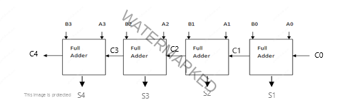
Binary Parallel Adder
The Binary Parallel Adder is a combinational circuit that adds two binary numbers in parallel form. It consists of multiple Full Adders connected in series, where the carry-out from one adder is connected to the carry-in of the next. This setup allows the addition of multi-bit numbers efficiently.
In practice, a Binary Parallel Adder can handle n-bit numbers by chaining n Full Adders together. This configuration ensures that each bit is added with its corresponding bit from the other number, along with any carry from the previous addition.
For more insights on digital circuit design, visit our article on Introduction to VLSI.
Carry Propagation Adder
The Carry Propagation Adder is a type of Binary Parallel Adder where the carry bit propagates sequentially through each Full Adder. This method, also known as the Ripple Carry Adder, is straightforward but can be slow for large bit-widths due to the cumulative delay caused by carry propagation.
In high-speed applications, the carry propagation delay becomes a significant factor. To mitigate this, advanced adders like the Look-Ahead Carry Adder have been developed, offering faster performance by predicting carry bits in advance.
In an n-bit Ripple Carry Adder, the minimum delay to produce the final result is proportional to the number of bits, making it inefficient for large n. This limitation has driven the development of faster adder architectures, ensuring optimal performance in modern digital systems.
Design Module
Below is the Verilog code for a Ripple Carry Adder using Full Adders:
module ripple_carry_adder(
    input [3:0] a,
    input [3:0] b,
    output [3:0] sum,
    output carry
    );

    wire w1, w2, w3;

    // Instantiate Full Adders
    fa fa0(sum[0], w1, a[0], b[0], 1'b0);
    fa fa1(sum[1], w2, a[1], b[1], w1);
    fa fa2(sum[2], w3, a[2], b[2], w2);
    fa fa3(sum[3], carry, a[3], b[3], w3);

    endmodule

// Full Adder Module
module fa(sum, carry_out, a, b, carry_in);
    output reg sum, carry_out;
    input a, b, carry_in;

    always @(*) begin
        sum = a ^ b ^ carry_in;
        carry_out = (a & b) | (b & carry_in) | (a & carry_in);
    end
endmodule
Test Bench
To test the Ripple Carry Adder, use the following test bench:
module ripple_carry_adder_tb;
    reg [3:0] a, b;
    wire [3:0] sum;
    wire carry;

    ripple_carry_adder dut(a, b, sum, carry);

    initial begin
        $monitor("A=%4b, B=%4b | Sum=%4b, Carry=%b", a, b, sum, carry);
        $dumpfile("ripple_carry_adder_tb.vcd");
        $dumpvars;

        // Test cases
        a = 4'b0000; b = 4'b0000; #100;
        a = 4'b0101; b = 4'b1010; #100;
        a = 4'b1111; b = 4'b0001; #100;
        a = 4'b0110; b = 4'b0100; #100;
    end
    endmodule
Carry Look Ahead Adder
The Carry Look Ahead Adder (CLA) addresses the speed limitations of ripple carry adders by precomputing carry signals. Unlike parallel adders, where each carry must propagate through all stages sequentially, a CLA computes carry signals in advance, significantly reducing delay and enhancing performance. This efficiency is particularly beneficial in high-speed processors and complex digital systems where rapid arithmetic operations are critical.
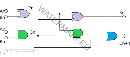
In a CLA, each bit pair generates two signals: Propagate (P) and Generate (G). These signals help in calculating the carry for each bit without waiting for the previous carry to propagate.
Propagation Term: Pn = An ⊕ Bn
Generate Term: Gn = An • Bn
The sum (S) and carry (C) are determined as follows:
Sum: Sn = Pn ⊕ Cn
Carry: Cn+1 = Gn + (Pn • Cn)
By cascading these equations, a 4-bit CLA can compute all carry signals simultaneously, drastically improving speed over ripple carry adders. However, this comes at the cost of increased circuit complexity.
Below is the block diagram of a four-bit CLA:
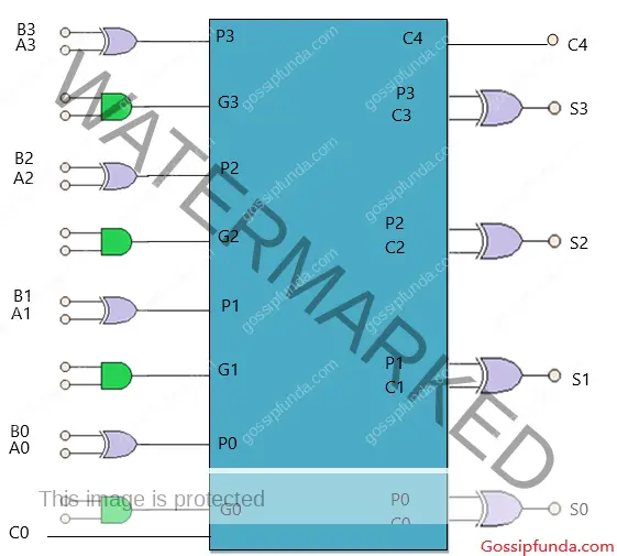
The carry equations for a 4-bit CLA are:
- C0 = Input Carry
- C1 = G0 + P0 • C0
- C2 = G1 + P1 • C1
- C3 = G2 + P2 • C2
- C4 = G3 + P3 • C3
The final carry out, C4, is computed using these equations, ensuring that all carry signals are generated in parallel, thus reducing the overall addition time.
Design
Here’s the Verilog implementation of a 4-bit Carry Look Ahead Adder:
// Combinational Circuits through Verilog
module carry_look_ahead(
    input [3:0] a, b,
    input cin,
    output [3:0] sum,
    output carry
);
    wire [3:0] p, g;
    wire [4:0] c;

    // Propagate and Generate
    assign p = a ^ b;
    assign g = a & b;

    // Carry equations
    assign c[0] = cin;
    assign c[1] = g[0] | (p[0] & c[0]);
    assign c[2] = g[1] | (p[1] & c[1]);
    assign c[3] = g[2] | (p[2] & c[2]);
    assign c[4] = g[3] | (p[3] & c[3]);

    // Sum equations
    assign sum = p ^ c[3:0];
    assign carry = c[4];
endmodule
This module efficiently calculates the sum and carry-out by leveraging the propagate and generate signals.
Test Bench
To verify the functionality of the Carry Look Ahead Adder, use the following test bench:
module testbench;
    reg [3:0] a, b;
    reg cin;
    wire [3:0] sum;
    wire carry;

    carry_look_ahead dut(a, b, cin, sum, carry);

    initial begin
        $monitor("Time=%0t | a=%d, b=%d, cin=%b | Sum=%d, Carry=%b", $time, a, b, cin, sum, carry);
        // Test cases
        a = 4'd0; b = 4'd0; cin = 0; #50;
        a = 4'd3; b = 4'd2; cin = 1; #50;
        a = 4'd7; b = 4'd10; cin = 0; #50;
        a = 4'd15; b = 4'd15; cin = 1; #50;
    end

    initial begin
        $dumpfile("carry_look_ahead_tb.vcd");
        $dumpvars;
    end
    endmodule

Difference between Serial and Parallel Adders
Understanding the distinction between serial and parallel adders is pivotal for selecting the right approach based on speed, complexity, and resource utilization. Here’s a comparative overview:
- Architecture:
- Parallel Adder: Utilizes multiple full adders, each handling a single bit of the input numbers simultaneously.
- Serial Adder: Uses a single full adder that processes one bit at a time, shifting through the bits sequentially.
- Speed:
- Parallel Adder: Faster as all bits are processed simultaneously.
- Serial Adder: Slower due to sequential processing of bits.
- Hardware Complexity:
- Parallel Adder: Requires more hardware resources (multiple adders and carry lines).
- Serial Adder: Simpler hardware with fewer components.
- Use Cases:
- Parallel Adder: Suitable for applications requiring high-speed arithmetic operations.
- Serial Adder: Ideal for resource-constrained environments where hardware simplicity is prioritized.
BCD Adder
The Binary Coded Decimal (BCD) Adder is designed to handle decimal digits encoded in binary form. Each decimal digit is represented by its 4-bit binary equivalent, making it easier to interface binary systems with human-readable decimal numbers.
For example, the decimal number 903 is represented in BCD as 1001 0000 0011.
BCD addition involves adding two BCD digits and adjusting the result if it exceeds 9 (1001 in binary). This adjustment ensures that each digit remains within the valid BCD range.
Logic
In BCD addition, after performing a standard 4-bit binary addition, the result is checked. If the sum exceeds 9, a correction factor of 6 (0110) is added to bring the sum back into the valid BCD range.
This process ensures that the resulting sum correctly represents a decimal number, preventing invalid BCD codes.
Design
Here’s the Verilog implementation of a 4-bit BCD Adder:
module BCD(
    output reg [3:0] sum,
    output reg cout,
    input [3:0] a, b
);
    reg [4:0] temp;

    always @(*) begin
        temp = a + b;
        if(temp > 4'd9) begin
            temp = temp + 4'd6;
            sum = temp[3:0];
            cout = temp[4];
        end else begin
            sum = temp[3:0];
            cout = 0;
        end
    end
endmodule
This module adds two 4-bit BCD digits and applies the necessary correction if the sum exceeds 9.
Test Bench
To verify the BCD Adder, use the following test bench:
module BCD_tb;
    reg [3:0] a, b;
    wire [3:0] sum;
    wire cout;

    BCD dut(sum, cout, a, b);

    initial begin
        $monitor("Time=%0t | a=%d, b=%d | Sum=%d, Carry=%b", $time, a, b, sum, cout);
        // Test cases
        a = 4'd2; b = 4'd9; #10;
        a = 4'd2; b = 4'd15; #10; // Note: 15 is invalid in BCD, to test correction
        a = 4'd1; b = 4'd6; #10;
    end

    initial begin
        $dumpfile("BCD_tb.vcd");
        $dumpvars;
    end
    endmodule

Excess-3 Adder
The Excess-3 Adder is utilized for adding two Excess-3 (XS3) code groups. In XS3, each decimal digit is represented by its corresponding 4-bit binary code plus 3 (0011). This encoding simplifies certain arithmetic operations and error detection mechanisms.
During addition, if there’s a carry, an additional 3 is added to the sum to maintain the XS3 encoding. Conversely, if there’s no carry, 3 is subtracted to correct the sum.
The design logic of an Excess-3 Adder mirrors that of a BCD Adder, with adjustments to the correction factor based on the carry signal.
Half Subtractor
A Half Subtractor is a combinational circuit that subtracts one binary digit from another, producing a difference and a borrow. It has two inputs, A (minuend) and B (subtrahend), and two outputs, Difference (D) and Borrow (BO).
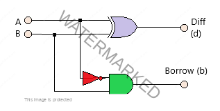
Analyzing the truth table, the Boolean expressions for the outputs are:
Difference: D = A’B + AB’ = A ⊕ B
Borrow: BO = A’ • B
Half subtractors can be implemented using only NAND or NOR gates, enhancing circuit flexibility and reusability.
Design
Here’s the Verilog implementation of a Half Subtractor:
module halfsub(
    output reg d,
    output reg bo,
    input a,
    input b
);
    assign d = a ^ b;
    assign bo = ~a & b;
endmodule
Test Bench
To verify the Half Subtractor, use the following test bench:
module halfsub_tb;
    reg a, b;
    wire d, bo;

    halfsub dut(d, bo, a, b);

    initial begin
        $monitor("Time=%0t | a=%b, b=%b | Difference=%b, Borrow=%b", $time, a, b, d, bo);
        // Test cases
        a = 0; b = 0; #100;
        a = 0; b = 1; #100;
        a = 1; b = 0; #100;
        a = 1; b = 1; #100;
    end

    initial begin
        $dumpfile("halfsub_tb.vcd");
        $dumpvars;
    end
    endmodule

Full Subtractor
A Full Subtractor extends the functionality of the Half Subtractor by considering an additional input, typically a borrow from a previous stage. It subtracts two bits, A and B, along with a borrow-in (C), producing a difference (D) and a borrow-out (BO).
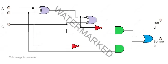
From the truth table, the Boolean expressions are:
Difference: D = A’B’C + A’BC’ + AB’C’ + ABC = A ⊕ B ⊕ C
Borrow: BO = A’C + A’B + BC
Implementing a Full Subtractor can be done using two Half Subtractors and an OR gate, promoting design reusability and simplicity.
Design
Here’s the Verilog implementation of a Full Subtractor:
module fs(
    output reg diff,
    output reg borrow,
    input a,
    input b,
    input c
);
    assign diff = a ^ b ^ c;
    assign borrow = (~a & c) | (~(a ^ b) & c);
endmodule
Test Bench
To verify the Full Subtractor, use the following test bench:
module fs_tb;
    reg a, b, c;
    wire difference, borrow;

    fs dut(difference, borrow, a, b, c);

    initial begin
        $monitor("Time=%0t | a=%b, b=%b, c=%b | Difference=%b, Borrow=%b", $time, a, b, c, difference, borrow);
        // Test cases
        a = 0; b = 0; c = 0; #100;
        a = 0; b = 0; c = 1; #100;
        a = 0; b = 1; c = 0; #100;
        a = 0; b = 1; c = 1; #100;
        a = 1; b = 0; c = 0; #100;
        a = 1; b = 0; c = 1; #100;
        a = 1; b = 1; c = 0; #100;
        a = 1; b = 1; c = 1; #100;
    end

    initial begin
        $dumpfile("full_subtractor_tb.vcd");
        $dumpvars;
    end
    endmodule

Conclusion
In this article, we’ve explored various Combinational Circuits through Verilog HDL, including Carry Look Ahead Adders, BCD Adders, Half Subtractors, and Full Subtractors. Understanding these circuits and their Verilog implementations is crucial for designing efficient digital systems and advancing in fields like VLSI. By mastering these concepts, you can create robust and high-performance digital circuits tailored to modern technological demands. Stay tuned to Gossipfunda for more comprehensive guides and the latest updates in digital electronics and circuit design.
Don’t Miss Our Previous Blogs
- Modeling Basic Gates through Verilog
- Modeling of Universal and Special Gates on Verilog
- Designing Combinational Circuits through Verilog HDL
- Modeling of Combinational Logic Circuits
I am an electronics and communication graduate. I qualified GATE in the same domain in 2019. Due to the appetite for VLSI, I am going to join the Hong Kong University of Science and Technology for Masters in IC design this year. My interest in writing evoked during college time when I wrote technical essays for college fest. Apart from it, I am a part of a few local NGOs too.


Really helpful, your way of writing really impressed me a lot.
You have quite good knowledge in combinational circuits.
Had you done any training in verilog, can you suggest me some good online classes.
Online course on Verilog by Maven Silicon turned out to be beneficial for me. I will recommend it.