Welcome to our comprehensive guide on Introduction to VLSI. If you’re passionate about electronics, understanding VLSI (Very Large-Scale Integration) is essential. VLSI technology has revolutionized the semiconductor industry, enabling the creation of complex integrated circuits that power everything from smartphones to supercomputers. In this article, we’ll delve into the history, design trends, advancements, and the reasons behind the widespread adoption of Integrated Circuits (ICs). Whether you’re a student, engineer, or tech enthusiast, this guide will provide you with valuable insights into the world of VLSI.
The reliance on electronic devices in consumer electronics, telecommunications, high-performance computing, and various other applications is growing rapidly. This cutting-edge technology offers unparalleled power and portability to end-users. The semiconductor industry has witnessed significant advancements over the past decades, primarily driven by enhanced designs, integration, and fabrication techniques.
History of Integrated Circuits
The semiconductor revolution began in 1947 with the invention of the transistor by researchers at Bell Telephone Laboratories. This breakthrough paved the way for the development of the Bipolar Junction Transistor, which became a cornerstone of the semiconductor industry. In 1958, Texas Instruments introduced the first Integrated Circuit (IC), integrating all necessary components—both active and passive—onto a single semiconductor wafer.
The 1960s marked a significant leap with the introduction of MOSFETs (Metal-Oxide-Semiconductor Field-Effect Transistors), which offered low power consumption and high-speed performance. These advancements laid the foundation for modern VLSI technology, enabling the creation of complex ICs used in calculators, microprocessors, and various digital devices.
Design Trends
As technology evolves, so does the complexity of IC designs. The demand for integrating more functions into smaller packages has driven the progression from Small Scale Integration (SSI) to Ultra Large Scale Integration (ULSI). Modern design trends focus on increasing transistor density, reducing power consumption, and enhancing performance. Innovations like 3D ICs and System on Chip (SoC) architectures are pushing the boundaries of what’s possible in VLSI design.
Don’t miss: Digital Circuit Design
Advancements in VLSI
Recent advancements in VLSI technology have focused on scaling down feature sizes, improving fabrication techniques, and integrating diverse functionalities into single chips. Wafer-Scale Integration (WSI) and 3D ICs are prime examples of how the industry is overcoming the limitations of traditional planar designs. Additionally, the rise of Artificial Intelligence (AI) chips and Internet of Things (IoT) devices has spurred the development of specialized VLSI architectures tailored for specific applications.
Why ICs Became Popular?
Integrated Circuits offer numerous advantages over discrete component designs:
- Compactness: ICs significantly reduce the size of electronic devices by integrating multiple components into a single chip.
- Low Power Consumption: Smaller circuits consume less power, making ICs ideal for battery-operated devices.
- High Speed: Shorter interconnects within ICs allow for faster signal transmission compared to discrete components.
- Cost-Effective: Mass production of ICs lowers the overall cost per unit, making advanced electronics more accessible.
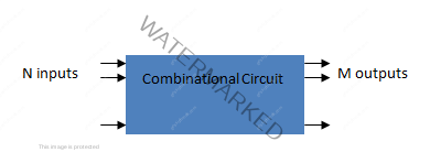
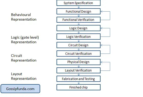
VLSI Design Flow
The VLSI design process is intricate and involves multiple stages to ensure the successful creation of complex integrated circuits. It typically follows a top-down and bottom-up approach, where high-level functionalities are broken down into smaller modules, and vice versa.
The Y-Chart
The Y-Chart illustrates the VLSI design flow across three primary dimensions: Behavioral, Structural, and Physical Layout. This framework helps designers navigate the complexities of creating efficient and reliable ICs.

The Y-Chart encompasses:
- Behavioral Design: Focuses on defining the functionality and behavior of the circuit using high-level descriptions.
- Structural Design: Involves organizing the circuit into interconnected modules and components.
- Physical Layout: Deals with the actual placement and routing of components on the silicon wafer.
Top-Down vs Bottom-Up Design
VLSI design employs both top-down and bottom-up methodologies to optimize performance and manage complexity. The top-down approach begins with a high-level specification, breaking it down into smaller, manageable modules. Conversely, the bottom-up approach starts with individual components, integrating them to form larger systems.
For example, designing an AI processor might start with defining its overall architecture (top-down) and then developing specialized units like tensor cores (bottom-up) to achieve the desired functionality.
Testability
Ensuring the reliability and functionality of VLSI designs is paramount. Testability refers to the ease with which a circuit can be tested for defects. Techniques like Design for Testability (DFT) and Built-In Self-Test (BIST) are employed to streamline the testing process, reducing time and costs while enhancing accuracy.
It’s crucial to incorporate testability early in the design phase to identify and rectify issues before fabrication. Ignoring this aspect can lead to costly recalls and reduced product reliability.
Conclusion
In this article, we’ve explored the Introduction to VLSI, tracing its history from the invention of the transistor to the latest advancements in integrated circuit technology. Understanding the evolution, design trends, and key advantages of ICs highlights why VLSI remains a cornerstone of modern electronics. As technology continues to advance, VLSI will play an increasingly vital role in shaping the future of digital devices and systems. Stay tuned to Gossipfunda for more in-depth guides and updates on the latest in electronics and VLSI technology.
I am an electronics and communication graduate. I qualified GATE in the same domain in 2019. Due to the appetite for VLSI, I am going to join the Hong Kong University of Science and Technology for Masters in IC design this year. My interest in writing evoked during college time when I wrote technical essays for college fest. Apart from it, I am a part of a few local NGOs too.


Comments are closed.