Digital electronics have the most comprehensive applications that mostly deal with calculations. Counters and Registers are the extensive utilization of a sequential circuit. Be it time-delay or pulse counting; these sequential circuit covers them all. This write-up is all about Counters and Registers.
Counters and Registers
We are going to explain both Counters and Registers one by one:
Registers
A register is a digital circuit with two primary functions, i.e., data storage and data movement. It is a group of flip-flops that logically connects to perform various tasks. To store a group of N-bit words we need ‘N’ flip-flops (one for each bit). We can also say that a register is a group of the binary warehouse that is fit for enduring binary data. Moreover, it may have combinational circuits for various data-related transactions.
The most straightforward possible register is the one that consists of only flip-flops without any external gate. The data enters in SERIAL (one bit at a time) or PARALLEL form (all the bits simultaneously)and can be retrieved in the serial or parallel form. Data in a serial form known as temporal code and data in an identical way as spatial code.
A register capable of shifting the binary information present into it from an external binary source is called the “shift register.” It is a sequential circuit mainly employed to store or move binary data either to the right (called right shift register) or to the left (called a left shift register).
Types of Register
The shift register can have a combination of serial and parallel shifter inputs and outputs including
Serial IN Serial OUT
Serial IN Parallel OUT
Parallel IN Serial OUT
Parallel IN Serial OUT
The SISO accepts the data serially, one bit at a time on a single input line and processes information on a separate line output. In ‘n’ bit register, to enter ‘n bit data, it requires ‘n clock pulses in serial form. The output requires (n-1) clock pulses to operate out.
In SIPO data records in serial form but output operates out in parallel. We can store n-bit serial input data in the ‘n’ number of the clock pulses. Whereas to take parallel output data, we need 0 number of clock pulses.
As the name suggests, PISO takes data parallelly and processes it serially. On the other hand, data input and output to PIPO is in parallel form. Another prototype, a Bi-Directional Shift Register, shifts the information (data) to the right and left both.
Universal Shift Register
A universal shift register is capable of doing all the operations like SISO, SIPO, PISO, PIPO and bidirectional shift. There are wide ranges of applications like time delay, data conversion, ring counter, sequence generator etc. Below are the design code and testbench, along with the simulation waveform.
Design and Test-bench
// Design
module usr(i,o,sir,sil,clk,s1,s0);
input [3:0] i;
input sir,sil,clk,s1,s0;
output reg [3:0] o;
wire [3:0] w;
mux_4x1 m1(w[0],s1,s0,i[0],sil,o[1],o[0]);
mux_4x1 m2(w[1],s1,s0,i[1],o[0],o[2],o[1]);
mux_4x1 m3(w[2],s1,s0,i[2],o[1],o[3],o[2]);
mux_4x1 m4(w[3],s1,s0,i[3],o[2],sir,o[3]);
D_ff d1(o[0],w[0],clk);
D_ff d2(o[1],w[1],clk);
D_ff d3(o[2],w[2],clk);
D_ff d4(o[3],w[3],clk);
endmodule
module D_ff(q,d,clk);
input d,clk;
output reg q;
always @ (posedge clk)
begin
q<= d;
end
endmodule
module mux_4x1 (y,a1,a0,i3,i2,i1,i0);
output reg y;
input a1,a0,i3,i2,i1,i0;
assign y= ((~a0)&(~a1)&i0) +((a0)&(~a1)&i1)+((~a0)&(a1)&i2)+((a0)&(a1)&i3);
endmodule
//Test
module usr_tb;
reg [3:0] i;
reg sir,sil,clk,s1,s0;
wire [3:0] o;
usr dut(i,o,sir,sil,clk,s1,s0);
always#50 clk=~clk;
initial
$monitor(i,o,sir,sil,clk,s1,s0);
initial
begin
clk=0;
sir=0;
sil=1;
i=4'b0000;
s1=0;
s0=0;
#100
i=4'b1010;
s1=0;
s0=1;
#100
i=4'b1111;
s1=1;
s0=0;
#100
s1=1;
s0=1;
end
initial
begin
$dumpfile("dump.vcd");
$dumpvars;
end
endmodule
Don’t miss: Designing Sequential Circuits through Verilog
Counter
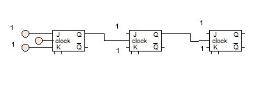
A counter is a digital circuit that counts the number of occurrences of input on clock pulses. Counters are a sequence of flip-flops. It also uses the combinational elements, along with the FFs, to generate control signals. Flip-flops are interconnected such that their combined state at any time is the binary equivalent of the total pulses that have occurred until that time. Below is a diagram of the 3-bit counter using J-K flip-flop.
Each count is a binary number known as the state of the counter. This counting is done in either a sequential manner or random manner to generate a specific sequence. Based on this counting direction, the counters are of four types: UP, DOWN, UP-DOWN and RANDOM.
Furthermore, there is one more sub-category: asynchronous and synchronous. In the asynchronous counter, there is no simultaneous clock pulse, whereas the sync pulse is available in the synchronous counter. A clock pulse triggers the first flip-flop of the circuit and then after each successive flip-flop clocks.
Up-Counter
Here, we are going to study about synchronous 4-bit UP counter. The UP counter is also known as the Ascending Counter as it follows an ascending increment pattern. Descending Counter is another name for DOWN counter.
A 4-bit UP counter consists of a series connection of 4 T flip-flops (or other flip flops converted into T flip-flops) Q0, Q1, Q2, Q3. The T flip-flop Q0 in the LSB position operates in Toggle Mode. The output of Q0 and Q1 undergo an AND operation and applies to Q2. Similarly, the production of Q2 and the produced output of Q0 and Q1 are further and-ed. Q3 further gets it. This construction satisfies the following necessary condition- A flip-flop in higher significant position toggles when the outputs of all lower significant flip-flops are equal to 1.
State transition condition are as follows
Q0 toggles on every clock pulse
Q1 toggles when Q0=1
Q2 toggles when Q0=Q1=1
Q3 toggles when Q0=Q1=Q2=1
Design and Test Bench
//Design
module up_counter(clk, reset, count);
input clk,reset;
output reg [3:0] count;
always@(posedge clk)
begin
if(reset)
count <= 4'b0000;
else
count <= count + 1;
end
endmodule
//Test
module up_countertb;
reg clk, reset;
wire [3:0] count;
up_counter dut(clk,reset,count);
initial
begin
$dumpfile("dump.vcd");
$dumpvars;
end
always #50 clk=~clk;
always@(posedge clk)
begin
$display ("value is %d", count);
end
initial
begin
clk = 0;
reset = 1;
#500;
reset = 0;
#1000;
$finish;
end
endmodule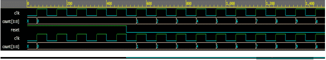
Synchronous Counter
The problem encountered with ripple counters is due to the accumulated FFs propagation delay. In other words, the FFs do not change states simultaneously in synchronism with the input pulses. The uses of synchronous counters or parallel counters subdue these limitations. In those counters, clock input pulses trigger flip-flops simultaneously.
Ring Counter
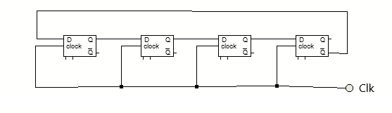
Ring Counter is the most straightforward shift register counter. It is also called the “end carry counter”. It is clear from the logic diagram that the Q output of each state connects to D input of the next state. However, the output Q0 of LSB is linking back to the input D3 of MSB FF. Each on the array of FFs is in a pattern of a ring and, hence, the name “ring counter.”
In this, only one bit is high and circulates the register as long as clock pulses are available. As the sequence repeats itself after four clock pulses; thus, the number of distinct states in the ring counter is equal to the number of FFs used in the counter. Therefore, with flip flops, there are n-states present in the ring counter MOD-M =n. Below are the design and testbench.
//Design
module ring_count(q,clk,clr);
input clk,clr;
output [3:0]q;
reg [3:0]q;
always @(posedge clk or posedge clr)
if(clr)
begin
q<=4'b0001;
end
else
begin
q[3]<=q[0];
q[2]<=q[3];
q[1]<=q[2];
q[0]<=q[1];
end
endmodule
//Test
module ring_count_test();
reg clk,clr;
wire [3:0]q;
ring_count dut1(q,clk,clr);
initial
begin
$monitor(q,clk,clr);
$dumpfile("dump.vcd");
$dumpvars;
end
initial begin
clr=0;
#50 clr=1;
#100 clr=0;
end
always
begin
#50 clk=1;
#50 clk=0;
end
Johnson Counter
The Johnson counter is a SISO shift register. Its design provides feedback from the inverted output of the last FF to the input of the first flip-flop. It is also known as the Twisted ring counter, Mobies counter and Switch tail ring counter.
The logic diagram shows each stage links to the D input of the next step. However, the output of the end-stage and the data of the initial phase are tied together. Therefore, the name became a twisted ring counter. Below is the diagram.
The sequence repeats after every eighth clock pulse. Thus for FFs, there are 2n possible states.MOD-M= 2n. In typical “Johnson counter” with ‘n,’ flip-flops and the input frequency is ‘f,’ then the output frequency is f=2n.
When a counter enters into an unused state, it will persist in moving from one unused state to another and will never find its way to a used state. Thus, the counter suffers from the problem of “LOCKOUT.”
Design and Test Bench
//Design
module johnson_ctr (
input clk,
input rstn,
output reg [3:0] out
);
always @ (posedge clk) begin
if (!rstn)
out <= 1;
else begin
out[3] <= ~out[0];
for (int i = 0; i < 3; i=i+1) begin
out[i] <= out[i+1];
end
end
end
endmodule
//Test
module tb();
reg clk;
reg rstn;
wire [3:0] out;
johnson_ctr   u0 (.clk (clk),
.rstn (rstn),
.out (out));
always #10 clk = ~clk;
initial begin
{clk, rstn} <= 0;
$monitor(clk,rstn,out);
repeat (2) @(posedge clk);
rstn <= 1;
repeat (15) @(posedge clk);
$finish;
end
endmodule
See also: Designing Combinational Circuits through Verilog HDL
Conclusion
In this article “Counters and Registers“, we saw the construction and code of various counter and registers available in the repository of the sequential circuit. The registers are the base of applications like data conversion, arithmetic operation, time delay, etc. where counters find its use in analog to digital transformation, stepper motors, and control signal generation. It is advised to study sequential circuits thoroughly to excel in these topics.
I am an electronics and communication graduate. I qualified GATE in the same domain in 2019. Due to the appetite for VLSI, I am going to join the Hong Kong University of Science and Technology for Masters in IC design this year. My interest in writing evoked during college time when I wrote technical essays for college fest. Apart from it, I am a part of a few local NGOs too.